
Skip to content
Fairview Semiconductor

Purpose-Built Silicon
for Advanced AI.

Eliminating the 1,000W generality tax. Turnkey, air-cooled silicon-to-software platforms — unifying HBM4 memory and MPU compute from die to rack.

Stallion S10Gallium HBM4Glass Core2nm GAAFET
Scroll
50%Capture
Stack Value Capture
350WTarget
Air-cooled envelope
70%+Target
TCO envelope
On-prem
Sovereign inference
Product Ecosystem

From Silicon Dies to Turnkey Rack Systems.

Two flagship products. One unified architecture. Infinite AI scale.

Memory Chipset

Gallium HBM4 Architecture

Direct die-to-memory attach providing 16.0 TB/s throughput for data-intensive AI models and high-efficiency training clusters. The Gallium Series redefines what memory bandwidth means for next-generation AI infrastructure.
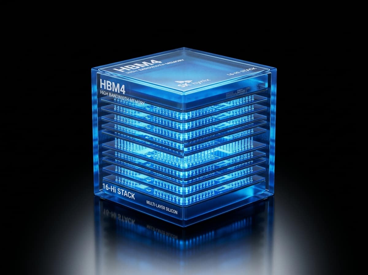
Bandwidth16.0+ TB/s
TechnologyHBM4 Stacked
Cubes4-Stack Flagship
Interface3Dx3D Heterogeneous Packaging (TSMC-SoIC + CoWoS-L)
Gallium HBM4 memory architecture — 4-stack HBM4 memory cube with 3Dx3D heterogeneous packaging
Gallium SeriesMemory Architecture
MPU Accelerator

Stallion AI Accelerator

2nm GAAFET (TSMC N2) compute die optimized for tensor execution and high-bandwidth memory access across dense AI infrastructure. The Stallion Series delivers unmatched parallel compute for LLM training, inference, and hyperscale AI workloads.
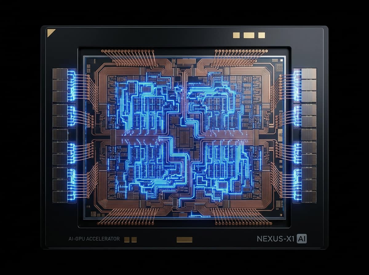
Compute0.15 PFLOPS FP32
Tensor Ops4.72 Dense PFLOPS (FP8 / FP4)
InterconnectPCIe 6 / CXL 3.2
Process Node2nm GAAFET (TSMC N2)
Stallion AI MPU compute die — 2nm GAAFET architecture with tensor execution units
Stallion SeriesMPU Compute Die
Next-Gen Silicon Architecture

High-Intensity AI Silicon

Stallion pairs programmable matrix execution with a wide-bus Gallium HBM4 interface in one package.

WORKLOAD-SPECIFIC COMPUTE

Stallionâ„¢ MPU

350W Pure Systolic Tensor Engine

350W air-cooled systolic tensor engines for deterministic inference.

SCALE-OUT INTERCONNECT

Galliumâ„¢ Fabric

Direct Zero-Copy Topology

Programmable scale-out interconnect with a direct memory-to-memory path, from a 2U blade to a rack.

EMERGING MEMORY

Tiered NVM Architecture

Near-Memory Data Access

Target architecture: tiered memory integration behind a technology-independent interface, with the physical memory cell qualified per node. Breaks the memory wall by optimizing near-memory data access for massive model parameters.

AI-OPTIMIZED STORAGE

KV-Cache Subsystem

High-Throughput Persistent Memory

High-throughput persistent storage subsystem engineered specifically for continuous agentic context memory and massive KV-cache retention, ensuring zero-latency recall for BFSI pipelines.

Architectural Paradigm

Package Architecture

Matrix Execution

Stallion assigns the die to programmable matrix execution and a wide memory interface.

Programmable Matrix Path

The matrix instruction set stays programmable across transformer, mixture-of-experts, and state-space workloads.

The Fairview Solution

Fairview Semiconductor re-architects compute from the transistor level up—combining maximum math-to-die density with programmable linear algebra primitives and next-generation wide-bus HBM4 integration.

Benchmarking

Stallion Architecture Summary

Design targets for the Stallion and Gallium package. Not measured silicon.

FeatureFairview Semiconductor
Math-to-Die AreaHigh (>35% flexible tensor execution)
Memory Architecture16,384-bit HBM4 Wide-Bus Interface
Model VersatilityHigh (Programmable Matrix ISA)
Sparsity AccelerationHardware-Native 2:4 Sparsity Decoding
Package BalanceBalanced Compute-to-Bandwidth Ratio
Enterprise Systems · 2027 Roadmap

1U, 2U & 3U High-Density Blade Servers.

FairView FV-RACK Series blade server datacenter rack — high-density AI compute infrastructure
FairView Systems · 2027 Delivery

FV-RACK Series

Unified MPU + HBM4 Compute Matrix

1U
Apex
32.768 TB/s
Aggregate BW
  • Compute4x Stallion S80I
  • Use CaseHigh-Density Inference & Edge
  • CoolingHigh-Static Air
  • NetworkDual 800GbE OSFP
Request Early Access
3U
Megascale
131.072 TB/s
Aggregate BW
  • Compute16x Stallion S80I
  • Use CaseRack-Scale Supercomputing
  • CoolingFull Liquid Immersion
  • Network8x 800GbE OSFP
Request Early Access
Regulated Microverticals

Purpose-Built for Sovereign & Enterprise Infrastructure.

Delivering dedicated, high-efficiency compute platforms tailored for regulated banking, sovereign national security, and high-availability enterprise infrastructure.

Regulated Banking (BFSI)

Algorithmic Trade Surveillance & Sovereign Core-Banking LLMs

Ultra-low latency, deterministic inference for algorithmic trade surveillance, AML monitoring, and sovereign core-banking LLMs executing directly on-premise without third-party API exposure.

BFSI MicroverticalDeterministic LatencyOn-Prem PII Compliance350W Air-Cooled
Request Engineering Attachment Specs for Regulated Banking (BFSI) →
Deterministic Inference Latency
< 1.2 ms
Compliance StandardAir-Gapped On-Premise PII Residency
Inference Latency< 1.2 ms (Zero-Jitter Execution)
Thermal Envelope350W Air-Cooled Standard Server Rack
Workload FocusAgentic LLMs & High-Frequency Risk Models
Advanced Packaging

The 3Dx3D Heterogeneous Glass Core Substrate.

Target co-packaged architecture (product family).

Shipping architecture is electrical: Stallion S10 MPU plus Gallium HBM4 over direct Cu-Cu hybrid bonding on a 3.2 ppm/K glass core substrate that ships with a reserved waveguide trench. FV-Link 4.0 co-packaged optics unlock in Phase 2 (Design Goal). All optical specifications are design targets pending PIC MPW validation.

DIRECT-TO-DIE AIR-COOLED HEATSINK (350W TDP)LIQUID METAL TIM · <0.04 °C/W THERMAL RESISTANCEHBM4HBM4HBM4HBM4HBM4HBM4HBM4HBM4STALLION S100TSMC 2nm GAAFET (TSMC N2) · 185B3Dx3D HETEROGENEOUS GLASS CORE SUBSTRATETHROUGH-GLASS VIAS (TGVs) · SUB-2µm RDL · 3.2 ppm/K CTE MATCH · ZERO WARPAGE
Interactive 3D Layer Cross-SectionActive: Stallion 2nm GAAFET (TSMC N2) Compute Die
Layer 2: Compute Core Engine
185B 2nm
Active Transistors

Stallion 2nm GAAFET (TSMC N2) Compute Die

Monolithic silicon die featuring 576 4th-Gen Sparse Systolic Tensor Engines and dedicated hardware transformer engines, interconnected via an on-die 2D Torus NoC mesh operating with zero inter-chiplet bridge latency penalties.

Process TechnologyTSMC 2nm GAAFET (TSMC N2) (N2P Platform)
Tensor Engines576 4th-Gen Sparse Cores
Dense FP8 Throughput4.72 Dense PFLOPS (FP8 / FP4)
Die-to-NoC InterconnectNon-Blocking 2D Torus Mesh
2nm GAAFET (TSMC N2)576 Systolic Tensor Engines185B Transistors4.72 Dense PFLOPS (FP8 / FP4)
Unified Architecture

Eliminating the Memory Wall.

From single silicon dies to datacenter racks — conventional AI architectures separate compute from memory, creating severe latency bottlenecks. FairView unifies high-throughput Stallion MPU dies directly with Gallium HBM4 memory on a single 2.5D substrate, scaling into turnkey enterprise blade systems for 2027–2028 deployments.

Compute Engine
4.72 Dense PFLOPS (FP8 / FP4)
FP8 Tensor Throughput

Silicon Compute Die (Stallion Series)

2nm GAAFET (TSMC N2) Architecture

185 billion transistors engineered for dense tensor operations and sparse matrix calculations, eliminating idle clock cycles with hardware transformer engines.

2nm GAAFET (TSMC N2)576 Systolic Tensor Engines185B Transistors
Memory Substrate
16.0 TB/s
Sustained Memory Bandwidth

Direct Memory Substrate (Gallium Series)

HBM4 TSMC-SoIC Direct Cu-Cu Attach

Direct die-to-memory attach across a 16,384-bit bus. The 16.0 TB/s figure is a design target for the Gallium subsystem.

16,384-bit Bus512 GB Capacity16-Hi DRAM
Package Integration
< 8 ns
Direct Substrate Latency

3Dx3D Glass Core Package Integration

Zero Memory Bottlenecks

Stallion and Gallium are co-designed on a Glass Core Substrate with TSMC-SoIC direct Cu-Cu hybrid bonding (<1µm pitch). Compute and memory operate as a single unified engine at 99% bandwidth efficiency.

Glass Core SubstrateDirect Cu-Cu (<1µm)Zero Warpage
2027–2028 Delivery
131 TB/s
3U Aggregate Throughput

Enterprise Rack Systems (Roadmap)

FV-RACK Series Systems

Turnkey 1U Apex, 2U Enterprise, and 3U Megascale blade servers with liquid-assisted rack cooling — each Stallion S100 running 350 W air-cooled — and PCIe Gen6 / CXL 3.2 fabrics designed for hyperscale AI cluster deployments.

1U / 2U / 3U BladesLiquid CooledCXL 3.2 Fabric

Unified Architecture Execution Pipeline

Stallion Compute Die
2nm GAAFET (TSMC N2) · 4.72 Dense PFLOPS (FP8 / FP4)
⟷3Dx3D Heterogeneous Packaging (TSMC-SoIC + CoWoS-L) Interposer (<8ns)
Gallium HBM4 Memory
16.0 TB/s Direct Attach
⟶CXL 3.2 / PCIe Gen6 Fabric
FV-RACK Systems
2027–2028 Delivery (1U/2U/3U)
Enterprise & Hyperscale Access

Request Early Access & Technical Datasheets.

Direct engagement for Stallion MPU silicon samples, Gallium HBM4 pinout specs, and official engineering datasheets.

Corporate (@domain.com) or Institutional (.edu) required for NDA datasheets
Dispatched to info@fairviewsemi.com · Confidential Silicon NDA
Inspect Stallion MPU Specs →Inspect Gallium HBM4 Specs →Download Brand Kit →
Fairview Semiconductor: AI Accelerator Silicon